Posted on 01/17/2019 10:56:19 AM PST by Red Badger
Researchers have created a field-effect transistor using a single-crystal, “paint-on” perovskite
Illustration: North Carolina State University
===================================================================
Transistors, and the conductive traces that connect them, are routinely created by the billions on the surface of silicon wafers, which are later cut into the individual “chips” that power our computers, phones, watches, and countless other electronic gadgets. But few people think much about how those silicon wafers are made in the first place. It’s quite tricky.
Very pure sand (silicon dioxide) has to be melted, at which point a seed crystal of elemental silicon is brought in contact with the melt, which slowly deposits silicon atoms on the seed, ones that extend the seed’s crystalline lattice. Masses of pure silicon are slowly grown this way, with an entire ingot, which might measure 30 centimeters or more in diameter, being one big well-oriented crystal. Such silicon ingots are then sliced thinly into wafers and polished, providing a substrate on which to build circuits made up of huge numbers of transistors, diodes, and other electronic devices.
No wonder electrical engineers have long sought easier ways to create the substrate on which to form their creations. Since the early 2000s, they've been able to produce transistors and similar devices using thin films of silicon and other semiconducting materials applied to insulating substrates. But that, too, requires rather complicated manufacturing techniques, often involving a high vacuum.
Another approach that has shown great promise in recent years is solution-processing of semiconductors. This is possible, for example with a class of hybrid organic-inorganic materials that have crystal structures matching that of the mineral perovskite. Such perovskite semiconductors can be formed simply by coating, say, a piece of glass with the proper chemical solution and letting it dry.
This approach has been used, in particular, to produce some remarkably efficient photovoltaic cells, ones that can compete with traditional silicon solar cells. It’s also been used to create perovskite-based photodetectors and light-emitting diodes.
Engineers are now extending the application of these easily fabricated perovskite semiconductors into a new realm: field-effect transistors. An international team led by Aram Amassian at North Carolina State University in Raleigh, N.C., has for the first time demonstrated the construction of field-effect transistors using a single crystal, hybrid perovskite semiconductor. A report of their work appeared on 17 December in the open-access journal Nature Communications.
While the design of perovskite solar cells has matured to the point of commercialization, making hybrid perovskites function as field-effect transistors has been much more of a challenge. That reflects the fact that perovskite films typically consist of multiple crystals with random orientations. Such polycrystalline materials include grain boundaries and various kinds of defects in their atomic crystal lattices, which limit how well charge carriers (electrons or “holes”) can move through them.
For a thin-film solar cell, polycrystalline perovskites can suffice, because charge carriers have to move only a few hundred nanometers up and down through the thickness of the material. But in a field-effect transistor of a size you can imagine printing, charge carriers would have to travel greater distances. Making the transistor from a single-crystal semiconductor thus works much better.
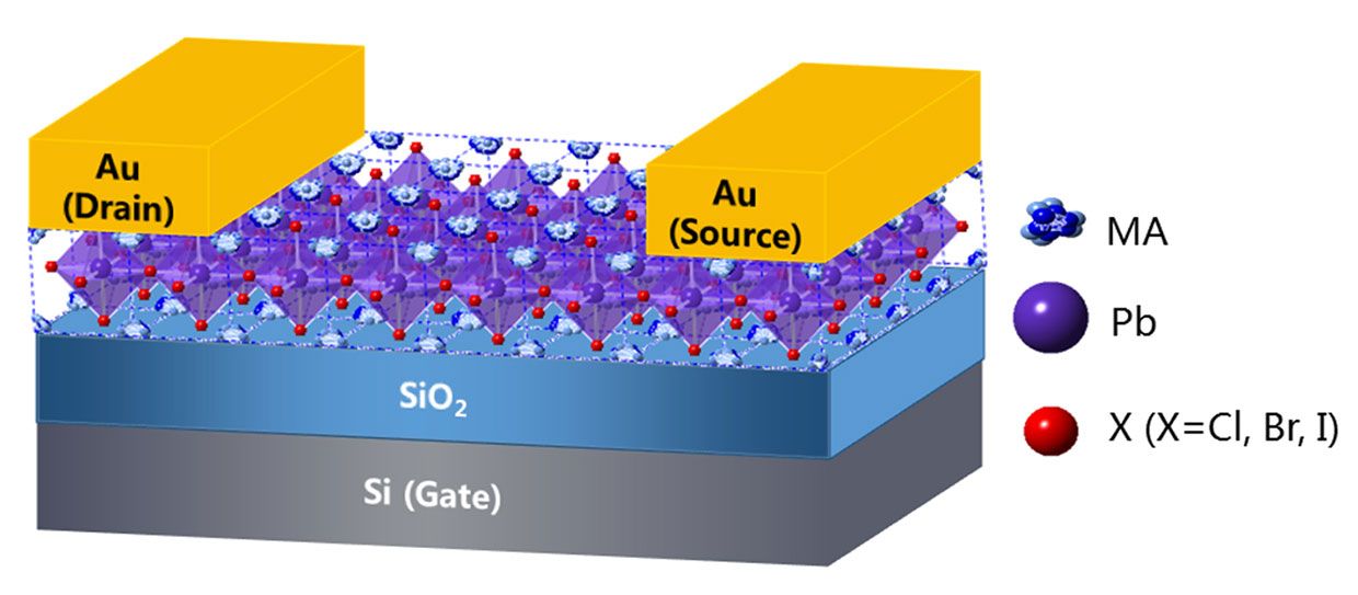
There are techniques that allow perovskite single crystals to be formed, but those crystals typically end up with defects on their surfaces, which makes it difficult to add the necessary electrical contacts. Amassian and his colleagues dodged that problem by fabricating a 2.5-micrometer-thick single perovskite crystal from a solution injected between two flat surfaces separated by a thin spacer—creating a perovskite “sandwich,” as it were.
The top surface included two gold electrical contacts, which functioned as the transistor’s source and drain. The bottom one in this experimental prototype, made of silicon covered by silicon dioxide, served as the transistor’s gate and gate insulator.
So the FET created by Amassian’s team still relies on a silicon substrate. But Amassian explains that they used silicon just to make their pioneering work a bit easier: Other materials, including glass or plastics, for example, could also be used.
The transistors they created in this way required 5 to 10 volts to be applied to the gate to fully turn on, more than any respectable field-effect transistor would need. That’s not fundamental to the perovskite material used, though; it’s just a function of the rather crude geometry of the early experimental units, Amassian explains.
There’s still a long way to go before useful commercial devices of this type can be fabricated. So don’t expect to be printing up perovskite electronics in your garage just yet. Still, this work makes a significant step toward just such a future.
Tech Ping!........................
“Creating a perovskites ‘sandwich’”
I like mine with a slice or two of American cheese.
Fascinating
Yummy.
Easily handled in the semiconductor industry, though. Building this stuff on plastics again raises the possibility of flexible circuits ... could greatly facilitate embedded controls.
That’s what’s in American cheese?
Back to peanut butter.
There’s still a long way to go before useful commercial devices of this type can be fabricated.
...
But they’ll do an article on it anyway, and put the important info at the bottom.
That’s what’s in perovskites. American “cheese” is probably worse.

Ahhhhh.....so they could make transistors out of American cheese.
Cows....making tasty food and fueling electronics.
Sounds very interesting...can envision a whole new kind of fab with less expensive machinery and more forgiving processes
American “cheese” is essentially plastic ... might be used for a flexible substrate.
Too late.
I already applied for the patent and started a partnership with Kraft.
Interesting as a concept but things are moving so fast in Semiconductors that no one is going to stop long enough to study it.
5-10nm design rules are taking all of the worlds resources to create functional designs which don’t bankrupt the companies doing them.
We are getting VERY close to the edge of impossibility even using EUV lithography.
Mmmmm, perovskites! Love fish, but Mrs. Thinking doesn’t.
Soon you will be placing individual atoms as building blocks................
Here's a good place to start: The Top Printed Electronics Blogs: 51 of the Best Blogs, Online News Sources and Publications on Printed Electronics Technologies, May 31, 2017 by Shelly Stazzone.

Thanks. The article does mention that there’s been success with printed solar cells.
But the research mentioned in the article about FET’s isn’t worthy of a news article at this time and probably not any time soon.
Then there’s the flash-tube from hell that turns the surface of a wafer molten for just an instant—anneals the surface without dispersing the dopant implanted just a wee bit deeper.
Disclaimer: Opinions posted on Free Republic are those of the individual posters and do not necessarily represent the opinion of Free Republic or its management. All materials posted herein are protected by copyright law and the exemption for fair use of copyrighted works.