 PCstats is going to take a quick look at what's currently known about the architecture of the Cell processor and its potential as a rival to today's x86-based 32 and 64-bit processors.
 Posted on 02/16/2005 8:23:30 PM PST by Ernest_at_the_Beach
IBM, in cooperation with fellow industry giants Sony and Toshiba, recently announced a new processor, called the Cell. While this in itself is not really cause for much celebration (except perhaps for the odd bedfellows involved in the project) the new multi-core chip might well prove to be something special. For one thing, it's going to be at the heart of Sony's upcoming Playstation 3 console, which we have a feeling may be slightly popular…
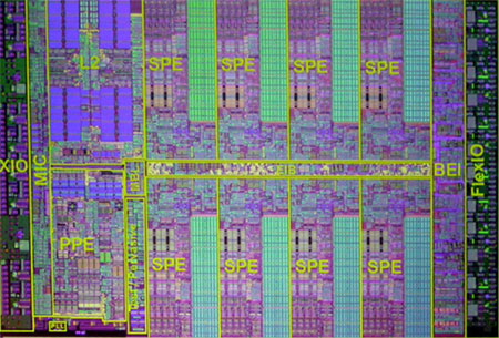
The Cell processor is vastly different from conventional processors inside. This tiny chip contains a powerful 64-bit Dual-threaded IBM PowerPC core but also eight proprietary 'Synergistic Processing Elements' (SPEs), essentially eight more highly specialized mini-computers on the same die.
It's these SPEs that make the Cell architecture special, as you might guess. IBM describes the product as a 'System on a Chip.' Like IBM's Power5 processors, multi-processing is build right into the die.
PCstats is going to take a quick look at what's currently known about the architecture of the Cell processor and its potential as a rival to today's x86-based 32 and 64-bit processors.
The basics: Cell Biology
As we mentioned, the prototype Cell processor is composed of a single 64-bit RISC PowerPC processor and eight SPE 32-bit units. These are bound together by a fast internal bus, the Elemental Interface Bus (EIB). A built-in dual channel memory controller is included, and connects to a current maximum of 256MB of extremely fast Rambus XDR memory. Communication with the rest of the system is provided by the FlexIO bus. This interface also allows high speed, chip-to-chip communication between different Cell processors, either inside or outside the same computer system.
The prototype Cell processor ran at 4GHz, and according to IBM, is capable of a theoretical maximum of 256Gflops, thus placing it instantly at the forefront of potential multi-chip supercomputer designs of the future. The chip is built on a 90nm process and contains 234 million transistors.
The Cell is allegedly capable of dynamic power management (perhaps a variant of Transmeta'a Long Run power management technology?), throttling itself to suit the current processing load. Internal temperature sensors are also present as you would anticipate.
The Synergistic Processing Elements: Cellular Engines
Each 'Synergistic Processing Elements' (SPE) is a powerful processor in its own right, focused on one thing: churning through single precision and double precision mathematical calculations. As each SPE component is a subordinate part of the whole Cell processor, they can dispense with a lot of the complex instruction queuing logic that a typical modern single processor computer needs. Each SPE gets its orders from the 64-bit Power PC unit which handles the scheduling and parceling of data out to the SPEs. Instead the focus is on speed.

Each SPE has 256KB of on-die memory allotted only to it, but instead of being used as conventional cache memory, this small area of high-speed storage is actually addressed almost like typical system RAM. The L1 cache memory found in conventional processors is highly automated, making it simple to program for but adding overhead. With the Cell processor, programmers can dictate exactly how they wish their software to use the 256KB allotment available to each SPE. This allows execution efficiency to be increased with good software design. It also allows better memory management and security from buffer overflows and other exploits.
Individual SPEs should be able to pass data to each other by storing it in specific areas of the system memory, forming a chain of processing units each performing a different operation on the data. Obviously this requires an extremely fast interface between the system RAM and the SPEs, which the Cell has in spades… More on this later.
The Element Interface Bus: Cellular Network
The SPEs are connected to each other and the Power PC 'brains' of the Cell by means of an 'Element Interface Bus' (EIB); this set of four 128-bit wide data channels also connects to the L2 cache memory and to the Memory Interface Controller and FlexIO 'front side bus' to pass data outside the chip. The EIB is a circular bus with two channel 'rings' traveling in opposite directions between and through the elements of the Cell processor.

The PowerPC Processing Element
This remains a bit of a mystery, as significant details of the operation of this processor have not yet been revealed by IBM and the partnership. What is known is that the 'main' Cell processor is a 64-bit chip that supports dual-threaded (SMT) operation, using a 32KB L1 cache and a 512KB level 2 cache.
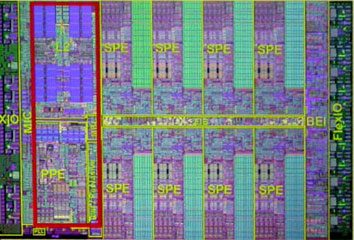
Most likely, the PowerPC Processing Element (PPE) will act as the controller, receiving, synchronizing and translating data 'jobs' and parceling them out to one or more of the SPEs for processing. Given that it's a powerful processor in its own right, the PPE may also lend its muscle to the number crunching also.
Memory Interface Controller (MIC) and FlexIO: Communicating Outside the Cell
The Memory Interface Controller connects to the EIB and passes data to and from main memory. It's built into the die of the Cell processor, similar to the approach taken by AMD with its 64-bit Opteron and Athlon 64 processors. The IBM MIC is connected to dual channels of Rambus (yes that name again) XDR memory. Total bandwidth should be in the area of 25GB/s. The Cell needs a fast memory interface to handle the data it's capable of spewing out.
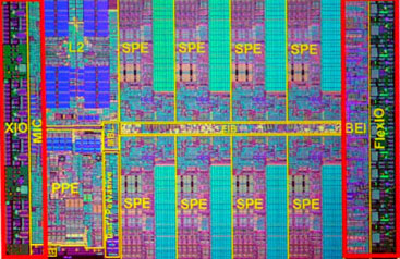
The connection between the Cell chip and the rest of the system will be handled by the proprietary 'FlexIO' bus, providing a daunting 76.8GB/s maximum bandwidth. This huge number is broken up considerably by the fact that the ingoing and outgoing data handling capacity of this bus is split into two parts; 'coherent' data traffic intended for transmission to other Cell processors and 'non-coherent' traffic intended for the rest of the system as in a typical 'front side bus' arrangement.
Beyond Playstation 3: The future of the Cell?
One of the most interesting properties of this new processor is its modular design. In addition to being essentially a multi-processor solution on a chip, each Cell processor can theoretically share its processing tasks with any other Cell processor anywhere, not just ones hooked up to the same system.
Imagine a 'world of tomorrow' where the Cell-based processors in your TV and your toaster quite happily help your Playstation V chew through some advanced weather physics calculations while you watch your collection of blu-Ray DVDs… call it 'SkyNet'. ;-)
Back to earth. Obviously the idea of this sort of communication is still just potential, but the Cell's architecture really does allow for this sort of out-of-box co-processing-cooperation. Of course, for it to be at all useful, better networking technologies will need to placed in production. Infiniband, anyone?
More SPEs?

Cell core and CPU photos courtesy of PCwatch.co.jp
The way that the Element Interconnect Bus is designed allows for more than the eight SPEs shown in IBM's prototype Cell chip.
It would also allow for less...
The potential here for a range of Cell based designs to cover all sorts of processing requirements is obvious.
Overall, the IBM/Sony/Toshiba Cell processor has a bright future ahead of it, and not just because millions will be sold in Playstation 3 consoles. With the correct compiling tools, Cell-inside PCs could potentially excel at the kind of applications we buy high-end PCs for today: Graphics,
video, audio and games.
The only question that remains is will they in the face of Intel's upcoming Extended Memory-64 Technology and dual-core Pentium 4 processors?
Find out about this and many other reviews by joining the Weekly PCstats.com Newsletter today! Catch all of PCstats latest hardware reviews right here.
ping
Very interesting! Thanks for posting the data & the graphics.
Interesting article with some facts and also some breathless hype. Can programs be written to exploit the parallelism that is present on the chip? Will new programming languages need to come along to further this end? These are unanswered questions. Also not mentioned in the article (I don't think) is something I read elsewhere which is that the "cells" receive chunks of both code and data - something that doesn't really happen in a conventional chip.
New Chip to Challenge Intel (Cell processor from IBM Sony Toshiba)
Uhhh... it's hype ... programming model is quite difficult to handle and utilize fully... it's what has stymied parallel processing for 25 years.
The SPE's are really "Like" miniature Cray processors.
No virtual memory, raw speed, floating point attached processors.
HUH?
Sure but you've got to find and exploit the parallelism. Read an article the other day - one place there is nearly perfect parallelism is in compilation - these machines would probably make good build machines.
See this for photos of what is being done with current hardware ( probably for video editing ):
AMD Dual-Core Demonstrations Get Two Thumbs Up At Linuxworld
Lots of programming to be done.
wrt parallel processing: IS your PC a SIMD Connection Machine? Or a 256 processor Sequent-like shared memory machine? Or a vector machine? Yet all those machines used fewer transistors than you have
in your PC today, even though they have more raw power on a MIPS/transistor scale. They arent used because your PC software cant utilize them. Same here.
This architecture has been built before, and exists today in a number of ASSPs. it has utility in certain areas, but to think it will take over the world is HYPE.
JMHO.
Some compilers are attempting to automatically generate code from common languages like "C" to take advantage of parallel execution.
On Macs, we can write SIMD vector processing code for G4 and G5 processors using "C"-type languages. And we can use multiple CPUs, so coarse-grained and fine-grained parallelism are available together.
A few specialized programming languages exist to better utilize parallelism. Some time ago, I learned a language called "Occam" for a processor called the "Transputer". The language was simple, but designing code that avoids deadlocks, livelocks, race conditions, etc. requires a lot of effort. Computers could contain multiple Transputer chips, and Occam would automatically distribute the processing and handle the communications between each chip. If I recall correctly, each Transputer had four built-in serial communication paths, so grid topologies could be easily designed.
Disclaimer: Opinions posted on Free Republic are those of the individual posters and do not necessarily represent the opinion of Free Republic or its management. All materials posted herein are protected by copyright law and the exemption for fair use of copyrighted works.