
"There's far too much graphene violins on FR."
Posted on 04/22/2008 8:03:54 AM PDT by RightWhale
Manchester, UK (SPX) Apr 22, 2008
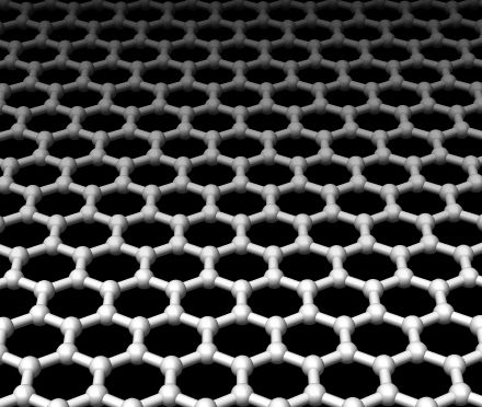
Researchers have used the world's thinnest material to create the world's smallest transistor, one atom thick and ten atoms wide. Reporting their peer-reviewed findings in the latest issue of the journal Science, Dr Kostya Novoselov and Professor Andre Geim from The School of Physics and Astronomy at The University of Manchester show that graphene can be carved into tiny electronic circuits with individual transistors having a size not much larger than that of a molecule.
The smaller the size of their transistors the better they perform, say the Manchester researchers.
In recent decades, manufacturers have crammed more and more components onto integrated circuits. As a result, the number of transistors and the power of these circuits have roughly doubled every two years. This has become known as Moore's Law.
But the speed of cramming is now noticeably decreasing, and further miniaturisation of electronics is to experience its most fundamental challenge in the next 10 to 20 years, according to the semiconductor industry roadmap.
At the heart of the problem is the poor stability of materials if shaped in elements smaller than 10 nanometres (1) in size. At this spatial scale, all semiconductors -- including silicon -- oxidise, decompose and uncontrollably migrate along surfaces like water droplets on a hot plate.
Four years ago, Geim and his colleagues discovered graphene, the first known one-atom-thick material which can be viewed as a plane of atoms pulled out from graphite. Graphene has rapidly become the hottest topic in physics and materials science.
Now the Manchester team has shown that it is possible to carve out nanometre-scale transistors from a single graphene crystal. Unlike all other known materials, graphene remains highly stable and conductive even when it is cut into devices one nanometre wide.
Graphene transistors start showing advantages and good performance at sizes below 10 nanometres - the miniaturization limit at which the Silicon technology is predicted to fail.
"Previously, researchers tried to use large molecules as individual transistors to create a new kind of electronic circuits. It is like a bit of chemistry added to computer engineering", says Novoselov. "Now one can think of designer molecules acting as transistors connected into designer computer architecture on the basis of the same material (graphene), and use the same fabrication approach that is currently used by semiconductor industry".
"It is too early to promise graphene supercomputers," adds Geim. "In our work, we relied on chance when making such small transistors. Unfortunately, no existing technology allows the cutting materials with true nanometre precision. But this is exactly the same challenge that all post-silicon electronics has to face. At least we now have a material that can meet such a challenge."
"Graphene is an exciting new material with unusual properties that are promising for nanoelectronics", comments Bob Westervelt, professor at Harvard University. "The future should be very interesting".
Whoa.
To quote Steve Martin:
“Lets get small!”
"There's far too much graphene violins on FR."
Me either ... EE chip designer ... former member of iPod / iPhone /iTouch chip design team ... former member of Motorola Razer phone / MAC G4 CPU chip design team ... former member Intel Centrino design team. Aren’t all Freepers ignorant knuckle draggers ?
What are the scientific units of this quantity, Rosanna?
It’s in “crams per second”. Fancy not knowing that.
In 45 nanometer myself. It’s getting really difficult to cram this stuff in there anymore. Actually, it’s more difficult getting it to work.
Intel seems to have it down.
How do you think 32 nm will work out?
It’s just mind boggling to us non-scientists. Can this thing even be seen by an electron microscope??
It seems to be even less materially speaking than spiderwebs.
Yea, right. They said silicon was at its limits back when I was in EE school in 1984. We were supposed to start shifting to GaAs. But we kept pushing Si beyond its "limits".
Yes they do. Our fab is not quite cutting edge.
Well, if you’re chasing 45 nm I hope you’re close to cutting edge.
Trying to think of who (besides a University) might be doing 45 nm in PA... can’t think of an IBM facility...
LSI?
Good guess.
Disclaimer: Opinions posted on Free Republic are those of the individual posters and do not necessarily represent the opinion of Free Republic or its management. All materials posted herein are protected by copyright law and the exemption for fair use of copyrighted works.